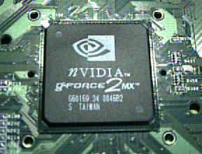
Nvidia GeForce2 MX
Introduction
I know it’s been a while since I churned out a review folks. Anyway, this time I got my hands on a board directly from Nvidia. Well NO, it’s not some surreptitious reference design I hid under my jacket when leaving their research lab, rather a good ol’ GeForce2 MX. Basically the GeForce2 MX fits in between the high-end (GeForce2 GTS & GeForce DDR) and low-end (Riva 128ZX, TNT, TNT2) products from Nvidia. Though it’s common to find avid gamers spending $500++ on video cards, not everybody sees it in the same light.
So that’s why Nvidia has come up with the GeForce2 MX chip, which is for the budget conscious folk among us. Initially when Nvidia launched the GeForce2 MX chip their main goal was to increase market share from 20% to 60% with their new product. So have they achieved this target? Well, don’t ask me; ask them, they’ll probably tell you. What we do here is tell you how good/bad the product is. (As if you didn’t know that already!)
Technology

The GeForce2 MX is a mix of aged and new technology, which sports state-of-the-art features like a hardware Transformation and Lighting (T&L) engine, a high-definition video processor, AGP 4x support, the new (NVIDIA Shading Rasterizer (NSR), and easy integration with Nvidia’s Detonator driver set. But it also still uses older SDRAM technology and 2 pixel pipeline (Nvidia’s GeForce2 GTS has a 4-pixel pipeline).
Specs:
0.18 micron core
175MHz core clock
166MHz memory clock
2 pixels per clock cycle
350 Mpixels/s fill rate
4 texels per clock cycle
700 Mtexels/s fill rate
2.7 GB/s memory bandwidth
20 million triangles/sec
8-64MB frame buffer
128-bit Single Data Rate (SDR) or 64-bit Double Data Rate (DDR) memory
TwinView architecture
Digital Vibrance control
Integrated Dual-Link TMDS transmitters
NVIDIA Shading Rasterizer (NSR)
High-Definition Video Processor (HDVP)
AGP 4X with Fast Writes
32-bit color
32-bit Z/stencil buffer
Cube environment mapping
DirectX and S3 texture compression
350MHz RAMDAC
GeForce2 GTS, GeForce2 MX essentials
Ok let’s get the nuts & bolts figured out before going any further.
The GeForce2 GTS could push out four pixels per clock and is able to process two textures per pixel pipeline for 8 texels per clock. The GeForce 2 MX only has a dual-pixel pipeline, but retains the GeForce2 GTS’s ability to process two textures per clock.
This makes you think the MX should have half the pixel fill rate of the GeForce2 GTS, right? Wrong. The difference comes with each chip’s different clock speed. The GeForce2 GTS has a 200MHz clock, which results in an 800 Mpixels/s fill rate (4 pixels per clock x 200MHz) and a 1.6 Gtexels/s fill rate (8 texels per clock x 200MHz).
Whereas the GeForce2 MX supports a 175MHz clock for fill rates of 350 Mpixels/s (2 pixels per clock x 175MHz) and 700 Mtexels/s (4 texels per clock x 175MHz).
The most appealing feature of the MX chip is the low wattage it requires. The chip uses only a meager 4 watts of power, allowing it to produce less overall heat and makes for less motherboard incompatibilities. Contrasting to practically every card on the market, the GeForce2 MX cards don’t require active fan cooling, and some MX boards may even be shipped without heat sinks. Even the reference card we received lacks a heat sink. The lack of high-power requirements and its low heat emissions has made the chip very attractive for the mobile markets, although such features are desired on basic PC’s as well.